A Technical Introduction to Laser Diodes
Chapter 2
Principles of AlGaAs Laser Diodes
Author: Dr. Matthias Pospiech and Sha Liu
University of Hannover, Germany
Page Updated: October 22, 2019
In the double heterostructure, stimulated emission occurs only within a thin active layer of GaAs, which is sandwiched between p- and n- doped AlGaAs layers that have a wider band gap. Laser diodes use heterojunctions to achieve simultaneous carrier and photon confinement in the active region. A high laser efficiency demands that the light and injected charge carriers be confined as closely as possible to the same volume.
2.1 Heterostructure of a Laser Diode
Heterostructure of a laser diode
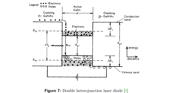
As illustrated in Figure 7, the AlGaAs Laser Diode consists of a double heterojunction formed by an undoped (or lightly p-doped) active region surrounded by higher bandgap p and n AlxGa1-xAs cladding layers. The surrounding cladding layers provide an energy barrier to confine carriers to the active region. The actual operation wavelengths may range from 750 - 880 nm due to the effects of dopants, the size of the active region, and the compositions of the active and cladding layers. When a certain parameter is fixed, the wavelength can vary in several nanometers due to other variables. For example, when the active layer has an energy gap Eg = 1.424 eV, the nominal emission wavelength is λ = hc/Eg = 871 nm. When a bias voltage is applied in the forward direction, electrons and holes are injected into the active layer. Since the band gap energy is larger in the cladding layers than in the active layer, the injected electrons and holes are prevented from diffusing across the junction by the potential barriers formed between the active layer and cladding layers (Figure 7). The electrons and holes confined to the active layer create a state of population inversion, allowing the amplification of light by stimulated emission. [9]
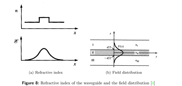
The cladding layers serve two functions. First, inject charge carriers. Second, light confinement. Since the active region has a smaller bandgap than the cladding layers, its refractive index will be slightly larger than that of the surrounding layers. The GaAs refractive index at these wavelengths is n = 3.5 while the refractive index of the AlxGa1-xAs cladding layers is slightly smaller. The Figure 8 indicates the electromagnetic field distribution due to the heterostructure.
laser diode electromagnetic field
For the confinement in the horizontal (lateral) direction, in real laser structures, index or gain guiding is always used, as mentioned in section 3.1.
The characteristics of a three-layer slab waveguide are conveniently described in terms of the normalized waveguide thickness D, defined as

where na and nc are the refractive indices of the active and cladding layers respectively and d is the active layer thickness.
The confinement factor Γ, defined as the fraction of the electromagnetic energy of the guided mode that exists within the active layer, is an important parameter representing the extent to the active layer. Γ for a fundamental mode is approximately given by [1]

2.2 Threshold Current
When a sufficient number of electrons and holes are accumulated to form an inverted population, the active region exhibits optical gain and can amplify electromagnetic waves passing through it, since stimulated emission overcomes interband absorption. The wave makes a full round trip in the cavity without attenuation, which means that the optical gain should equal the losses both inside the cavity and through the partially reflecting end facets. Thus, the gain coefficient at threshold gth is given by the relation

laser diode gain coefficient at threshold current point
Here, αa and αc denote the losses in the active and cladding layers respectively, due to free-carrier absorption. αs accounts for scattering loss due to heterointerfacial imperfections between the active and cladding layer. The first three loss terms on the right-hand side combined are termed internal loss αi and add up to 10 to 20 cm-1. The reflection loss 1/L ln 1/R ≈ 40 cm-1 for L ≈ 300mum, R = 0.3) due to output coupling is normally the largest among the loss terms.
There is a phenomenological linear relationship between the maximum gain g and the
injected carrier density n, supposing ![]() and nt are constant to a good approximation.
and nt are constant to a good approximation.

gain with injected current density
Here, ![]() is termed differential gain, and nt denotes the carrier density required to achieve transparency where stimulated emission balances against interband absorption
corresponding to the beginning of population inversion. Taking GaAs lasers
as an example,
is termed differential gain, and nt denotes the carrier density required to achieve transparency where stimulated emission balances against interband absorption
corresponding to the beginning of population inversion. Taking GaAs lasers
as an example, ![]() ≈ 3.5 x 10⁻⁶ cm2 and nt ≈ 1.5 x 1018 cm-3, and remember Γ=0.27, α=10cm-1 and L-1 ln R-1 = 40cm-1, we get a threshold carrier density n ≈ 2 x 1018cm-3. The threshold current density Jth is expressed as
≈ 3.5 x 10⁻⁶ cm2 and nt ≈ 1.5 x 1018 cm-3, and remember Γ=0.27, α=10cm-1 and L-1 ln R-1 = 40cm-1, we get a threshold carrier density n ≈ 2 x 1018cm-3. The threshold current density Jth is expressed as

where Ts is the carrier lifetime due to spontaneous emission. Assuming that Ts=3ns and d=0.1µm, we obtain a threshold current density Jth ≈ 1K Acm-2 [1]
2.3 Oscillation Modes
In laser diodes, length determines longitudinal modes where width and height of the cavity determines transverse or lateral modes.
longitudnal modes of a laser diode
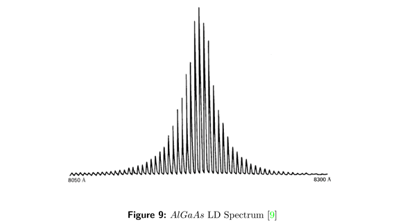
Longitudinal Mode: The longitudinal modes, or optical resonances of the Fabry-Perot formed by the cleaved facet end mirrors, are determined by the length L of the resonator and the refractive index n of the semiconductor. For electromagnetic wave of wavelength λ, the half-wavelength in the medium is λ/2n, and for a standing wave, qλ/2n = L, q is the integral multiple. Variation of the integer q by 1, causes a wavelength variation, Δλ of 0.35nm, and the laser resonator may simultaneously support several standing waves, or longitudinal modes, of slightly different wavelength. In a laser diode, the oscillation arises at the wavelength corresponding to the band gap energy of the semiconductor, the intensity decreases as the wavelength goes far away from the central wavelength, as indicated in Figure 9. Since the band gap energy varies with temperature, the wavelength with maximum intensity also varies with temperature. For example, the AlGaAs laser diode, the wavelength increases by approximately 0.23nm for an increase in temperature of 1 degree. The free spectral range ffsr is defined as

The peak separation is defined as

Figure 9 is an example with the center wavelength λ = 817.5 nm and the peak separation Δλ = 0.45 nm, the free spectral range ffsr = cΔλ/λ2 = 200GHz. [9]
index guided laser diode
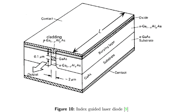
Transverse Modes: The transverse mode represents the state of the electromagnetic standing wave in the direction perpendicular to the optical axis of the laser resonator. The transverse mode has two components, one parallel and the other perpendicular to the active layer of the laser. As stated above, there exist steps in the refractive index on each side of the active layer, which serve to confine the light to the active layer. The laser beam displays a diverging field due to the diffraction at the ends of the cavity. Fig 10 shows the construction of a typical index guided laser diode with cladding layers, electrodes, and GaAs active region. The laser cavity mirrors are the end facets of the semiconductor crystal, which has been cleaved.
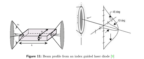
beam profile index guided laser diode
The dimensions of the crystal determine the pattern of the emitted beam (the transverse mode pattern) and also the possible laser emission frequencies (the longitudinal mode pattern). The output pattern is dominated by diffraction because the width W ≈ 10µm and height H ≈ 2µm of typical LDs are comparable to the emission wavelength. The divergence angle of the emission along these two directions is inversely proportional to the dimensions as shown in Fig 11. The angular width ϑ of the emission pattern from a slit or rectangular opening of width d is

divergence angle of a laser diode
For example, a laser wavelength of 850 nm and strip width W = 10µm has a divergence angle ϑw ≈ 10 deg, ϑH ≈ 45 deg as shown in Fig 11. The dimensions W and H of the active region of a laser diode can be determined by measuring the output emission cone angles. The smaller the aperture the greater the diffraction, with a sufficiently small W and H, only the lowest transverse mode TEM00 exits. [9]