A Technical Introduction to Laser Diodes
Chapter 3
Laser Diode Technology
Author: Dr. Matthias Pospiech and Sha Liu
University of Hannover, Germany
Page Updated: October 22, 2019
In the further proceedings we are going to take a closer look at different techniques of constructing a laser diode. The focus thereby is on single mode laser diodes. Single mode waves are preferred in most cases. The realm of multimode lasers are high power lasers, where single mode operating is not of importance.
3.1 Real Lasers
Most modern semiconductor lasers adopt a structure, where the current is injected only within a narrow region beneath a stripe contact several μm wide, in order to keep the threshold current low and to control the optical field distribution in the lateral direction. Compared with broad-area lasers, where the entire laser chip is excited, the threshold current of lasers with stripe geometry is reduced roughly proportional to the area of contact.
We differ mainly between two different types of structures. In case that the current injection is restricted to a small region along the junction plane these are termed gain-guided. Devices incorporating a built-in refractive index variation in the lateral direction are termed index-guided lasers. [1]
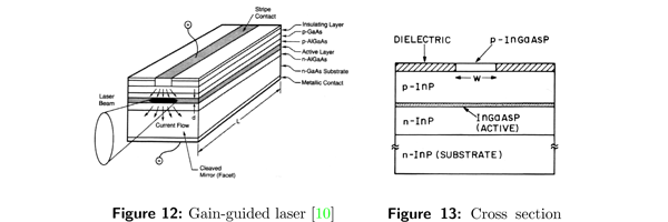
3.1.1 Gain-Guided Lasers
With these lasers the current injection is restricted to a narrow region beneath a stripe. The active region is planar and continuous. Lasing however occurs only in a limited region of the active layer beneath the stripe contact where high density of current flows. This horizontal confinement of the em–wave propagating through the active region is thereby accomplished by the small refractive index variation produced by the current generated population inversion. If the em–wave spreads in the horizontal plane outside of the horizontal dimensions of the stripe, it will be absorbed by the unexcited region of the active layer. In the vertical directions the lower refractive indices of the surrounding layers reflects the em–wave back into the active region. [11, 10]
The current restriction serves several purposes: [11]
- it allows CW operation with reasonable low threshold currents (10-100 mA)
- it can allow fundamental-mode operation along the junction plane, which is necessary for applications where the em–wave is coupled into a single mode optical fiber
- the requirements for heat sinking are low
gain guided laser diode cross-section
Such lasers are determined gain-guided lasers because the optical intensity distribution in the lateral direction is determined by the gain profile produced by carrier density distribution. [1]
3.1.2 Index-Guided Lasers
The transversal mode control in laser diodes can be achieved using index guiding along the junction plane. The mode control is necessary for improving the em–wave current linearity and the modulation response of lasers. The active region is thereby surrounded by materials with lower refractive indices in both the vertical (y) and lateral (x) transverse directions – the active region is buried in lower refractive indices layers (e.g. InP) on all sides. For this reason, these lasers are called buried-heterostructure lasers. [9,1]

index guided laser diode
The lateral index step along the junction plane is about two magnitudes larger than the carrier induced effects. As a result, the lasing characteristics of buried-heterostructure lasers are primarily determined by the rectangular waveguide that confines the mode inside the buried region. The transverse dimensions of the active region and the index discontinuities are chosen so that only the lowest order transverse modes can propagate in the waveguide. [9, 11]
These index guided devices produce beams with much higher beam quality, but are according to [10] typically limited in power to only a few hundred milliwatts. Another important feature of this laser is the confinement of the injected carriers to the active region. [9]
Buried Heterostructure Lasers: Figure 15 shows the schematic cross sections of different types of buried-heterostructure lasers. They are (i) the buried heterostructure that is also called etched-mesa buried-heterostructure (EMBH) to distinguish it from other BH lasers. And (ii) the double-channel planar buried heterostructure (DCPHB) laser. [11]
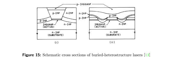
buried heterostructure laser diode cross-section
The fabrication of the EMBH structure is technologically complex and two epitaxial steps are necessary. Less critical is the DCPHB laser although this necessitate two epitaxial steps as well. There are other structures which are easier in fabrication, but these are not discussed here.
3.1.3 Gain vs. Index-Guided Structures
Historically, gain-guided devices based on the stripe geometry were developed first in view of their ease of fabrication. However gain-guided lasers exhibit higher threshold currents than index-guided lasers and have other undesirable characteristics that become worse as the laser wavelength increases. [11]
In contrast, the fabrication of strongly index-guided lasers requires either a single epitaxial growth over non-planar surfaces or two epitaxial growths and, in addition, careful attention to processing. In spite of these difficulties in fabrication, their superior performance characteristics – low threshold current, stable fundamental mode operation, and good high speed modulation characteristics – make them a prime candidate for high-performance applications. [11]
3.2 DBR and DFB Lasers
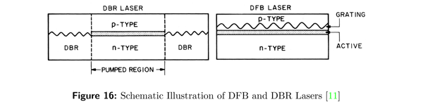
A standard Fabry Perot Laser diode is not wavelength selective. So the question is, how can wavelength selection can be achieved? Further decreasing the size of optical cavities creates difficulties beauase it becomes very difficult to manufacture smaller and smaller chips. Therefore, another method is to insert an optical feedback mechanism in the device to eliminate other frequencies and select a single frequency. Periodic gratings incorporated within the laser's waveguide can be utilized as a means of optical feedback. Devices incorporating the grating in the pumped region are referred to as Distributed Feedback DFB lasers », while those incorporating the grating in the passive region are termed Distributed Bragg Reflector (DBR) lasers.
DFB and DBR lasers oscillate in a single-longitudinal mode even under high-speed modulation, in contrast to Fabry-Perot lasers, which exhibit multiple-longitudinal mode oscillation when pulsed rapidly. [1]
Block drawing of a DFB laser diode
3.2.1 Distributed Bragg Reflector / DBR Lasers
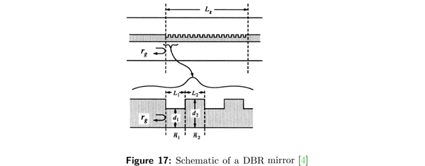
DBR mirrors: The gratings or distributed Bragg reflectors (DBRs) are used for one or both cavity mirrors. The grating thereby consist of corrugations with a periodic structure. They are used because of their frequency selectivity of a single axial mode. The period of grating is chosen as half of the average optical wavelength, which leads to a constructive interference between the reflected beams. Significant reflections can also occur in harmonic frequencies of the medium. The corrugations are typically etched on the surface of the waveguide, and these are re-filled with a different index material during a second growth. [4] This is illustrated in figure 17. The general concept of the grating is that multiple reflections will add up to a large net reflection. The reflections at the Bragg frequency add up to be exactly in phase. [4]
DBR laser diode mirror block diagram
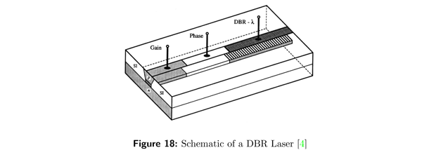
DBR Lasers: A DBR Laser can be formed by replacing one or both of the discrete laser mirrors with a passive grating reflector. Figure 18 shows a schematic of such a laser with one grating mirror. Besides the single frequency property provided by the frequency-selective grating mirrors, this laser can include wide tunability. Since the refractive index depends on the carrier density this can be exploited to vary the refractive index electro optically on the sections by separate electrodes.
The potential tunability of DBR Lasers is one of the main reasons why they are of great importance. As indicated in Figure 18, there are usually three sections, one active, one passive, and the passive grating. The first provides the gain, the second allows independent mode phase control and the grating is a mode selective filter. By applying a current or voltage the refractive index changes, shifting the axial modes of the cavity. [4, 1]
3.2.2 Distributed Feedback Laser ~ DFB Lasers
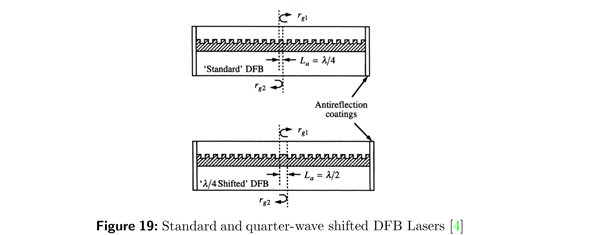
What is a DFB Laser? A distributed feedback laser (DFB) also uses grating mirrors, but the grating is included in the gain region. Reflections from the ends are suppressed by antireflection coatings. Thus, it is possible to make a laser from a single grating, although it is desirable to have at least a fraction of a wavelength shift near the center to facilitate lasing at the Bragg frequency. The idea behind this concept is, apart from the wavelength selectivity, to improve the quality of the laser, as the active length is a quarter-wavelength long. This applies for no shift in the gratings, where the cavity can be taken to be anywhere within the DFB, since all periods look the same. Here is a link to a list of DFB laser diodes »
DFB laser diode
For the standard DFB grating, we can see that the laser is antiresonant at the Bragg frequency. The modes of this laser are placed symmetrically around the Bragg frequency. However only the modes with lowest losses will lase. With a symmetrical gain profile around the Bragg frequency, this means that two modes are resonant.To suppress one mode we need to apply additional perturbation reflections, such as from uncoated cleaves at the end. An alternative method is to introducing an extra quarter wavelength element in the grating. This quarter wave shifted grating is shown in figure 19. This however is more difficult to fabricate. [12, 4]
3.2.3 DFB vs. DBR Lasers
DFB Lasers are easier to fabricate and show less losses and therefore have a lower threshold current. The DBR is widely tunable, but relatively complex since a lot of structure must be created along the surface of the wafer. for this reason DBR Lasers are only formed when their properties are required. Both lasers however work in single mode. [4]
3.3 High Power Laser Diode Arrays

high power laser diode
Semiconductor laser structures described so far have been developed for low power applications, such as providing a source in em–wave communication system. Their limitation in the output power mainly arises form the leakage current, which increases with an increase in the applied current. [11]
The major drawbacks of semiconductor lasers, the relatively low output powers, and the high beam divergence can be lowered by integrating multiple laser stripes into an array as shown in Figure 20. The stripes are closely spaced so that the radiation from neighboring stripes is coupled to form a coherent mode of the entire array to produce high power laser diodes. These laser diodes operate in multimode, in contrary to those described so far.
The array modes, often referred to as supermodes, are phaselocked combinations of the individual stripe modes and characterized by the phase relationship between the optical fields supported by adjacent stripes. [1]
high power VCSEL laser diode array
Laser arrays can be found in applications, where high beam powers and high beam densities are demanded. It therefore suggests itself for pumping of solid state lasers, because the wavelength range from 700 to 900 nm can be covered with appropriate semiconductor materials. [13]
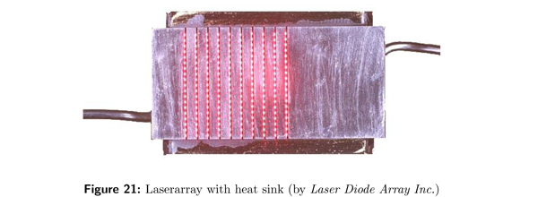
The one-dimensional arrays are also referred to as laserbars. Through stacking of these bars one can build up two-dimensional arrays. With such devices powers up to a few kW have already been achieved. [10]
3.4 VCSEL Vertical Cavity Surface Emitting Lasers
A vertical cavity surface emitting laser (VCSEL) is a specialized laser diode with improved efficiency and increased data speed. Older laser diodes, called edge-emitting diodes, emit coherent em–waves parallel to the boundaries between the semiconductor layers. The VCSEL emits its coherent em–waves perpendicular to the boundaries between the layers.
The VCSEL has several advantages over edge-emitting diodes. The VCSEL is cheaper to manufacture in quantity, is easier to test, and is more efficient. In addition, the VCSEL requires less electrical current to produce a given coherent energy output. The VCSEL emits a narrow, more nearly circular beam than traditional edge emitters. And because of its short cavity length it emits only one mode. [15]

VCSEL laser diode
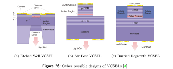
There are many designs of VCSEL structure however, they all have certain aspects in common. The cavity length of VCSELs is very short typically 1-3 wavelengths of the emitted em–wave. As a result, in a single pass of the cavity, a photon has a small chance of triggering a stimulated emission event at low carrier densities. Therefore, VCSELs require highly reflective mirrors to be efficient. In edge-emitting lasers, the reflectivity of the facets is about 30%. For VCSELs, the reflectivity required for low threshold currents is greater than 99.9%. Such a high reflectivity can not be achieved by the use of metallic mirrors. VCSELs make use of Distributed Bragg Reflectors. (DBRs) as described on page 17. These are formed by laying down alternating layers of semiconductor or dielectric materials with a difference in refractive index. Semiconductor materials used for DBRs have a small difference in refractive index therefore many periods are required. Since the DBR layers also carry the current in the device, more layers increase the resistance of the device therefore dissipation of heat may become a problem. [3]

As well as reducing the dimensions of the cavity one can reduce the threshold current of a VCSEL device by limiting the cross-sectional area in which gain occurs. There are a number of different types of lasers, which generally differ in the way in which high-reflectivity mirrors and current confinement is achieved.
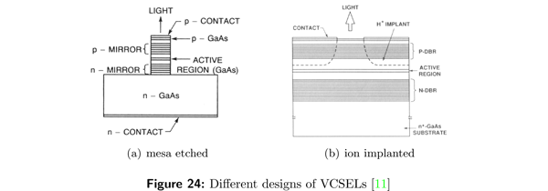
One simple method is to etch a pillar down to the active layer. These are termed mesa2 etched structure. Etched mesas are typically a few micrometer in diameter which allows fabrication of a large number of lasers on a single substrate. The large difference in refractive index between the air and device material also act to guide the em–wave emitted. However, for practical use a suitable bonding scheme is required. A polyamide can be used for filling up the region around the etched mesas, to allow a practical bonding scheme. Another problem with this type of structure are the loss of carriers due to surface recombination at the sidewalls and poor dissipation of heat from the laser cavity.
Another technique for current confinement is ion implantation. By selectively implanting ions into a semiconductor a region of high resistivity around a 10 µm diameter opening is produced. This scheme reduces current spreading, producing a region of high gain at the center of the opening where laser action takes place.
Since the substrate is absorbing in these cases, em–waves are emitted from the top. It can also be emitted from the bottom by using a structure in which the substrate near the emitting region has been etched away. [11, 3]

APPENDIX
Materials, wavelength and typical applications:
| GaN | AlGaAs/GaAs | InGaAsP/InP | AlGaAsSb/GaSb |
| 420-520nm | 780-870nm | 1300-1550nm | 1700-5000nm |
| blue-green | near infrared | near infrared | mid/far infrared |
| optical datastorage | optical transmission - short ranges | optical transimssion - long ranges | research |
Abbreviations:
This table provides a list of frequently used abbreviations in the subject of laser diodes:
| VB | Valance Band |
| CB | Conduction Band |
| SCL | Space Charge Layer |
| BH | Buried Heterostructure |
| CW | Continuous Wave |
| DBR | Distributed Bragg Reflector |
| DFB | Distributed Feedback Bragg |
| DHS | Double Heterostructure |
| LD | Laserdiode |
| MQW | Multiple Quantum Well |
| QW | Quantum Well |
| QC | Quantum Cascade |
| QD | Quantum Dot |
| VCSEL | Vertical Cavity Surface Emitting Laser |
List of Figures:
| p-n junction with/without bias [2] | Figure 1 |
| The carrier concentration in SCL under forward bias [2] | Figure 2 |
| Recombination [3] | Figure 3 |
| Electron and hole distribution [4] | Figure 4 |
| Recombination [5] | Figure 5 |
| Light feedback [3] | Figure 6 |
| Double heterojunction laser diode [9] | Figure 7 |
| Refractive index of the waveguide and the field distribution [4] | Figure 8 |
| AlGaAs LD Spectrum [9] | Figure 9 |
| Index guided laser diode [9] | Figure 10 |
| Beam profile from an index guided laser diode [9] | Figure 11 |
| Gain-guided laser [10] | Figure 12 |
| Cross section [11] | Figure 13 |
| Index-guided laser [9] | Figure 14 |
| Schematic cross sections of buried-heterostructure lasers [11] | Figure 15 |
| Schematic Illustration of DFB and DBR Lasers [11] | Figure 16 |
| Schematic of a DBR mirror [4] | Figure 17 |
| Schematic of a DBR Laser [4] | Figure 18 |
| Standard and quarter-wave shifted DFB Lasers [4] | Figure 19 |
| Laser diode array [1] | Figure 20 |
| Laserarray with heat sink (by Laser Diode Array Inc.) | Figure 21 |
| VCSEL laser diode Simulation [14] | Figure 22 |
| Layers of DBR mirrors | Figure 23 |
| Different designs of VCSELs [11] | Figure 24 |
| Etched Mesa | Figure 25 |
| Other possible designs of VCSELs [3] | Figure 26 |
References:
- [1] Nagaatsu Ogasawara. Lasers, semiconductor. Technical report, Nagaatsu Ogasawara University of Electro-Communications, www.pro-physik.de/Phy/pdfs/ OE042_1.pdf.
- [2] S.O.Kasap. Optoelectronics. Prentice Hall, 1 edition, 1999.
- [3] Carl Hepburn. Britneys guide to semiconductor physics. http://www.britneyspears.ac/lasers.htm.
- [4] Scott W. Corzine Larry A. Coldren. Diode Lasers and Photonic Integrated Circuits. John Wiley & Sons, 3 edition, 1995.
- [5] Mark Fox. Optical Properties of solids. Oxford University Press, 2001.
- [6] M. C. Teich B. E. A. Saleh. Fundamentals of Photonics. Wiley, New York, 1 edition, 1991.
- [7] Shane Eaton. Distributed Feedback Semiconductor Lasers.
- [8] DEPARTMENT OF PHYSICS and APPLIED PHYSICS. 3rd/4th year laboratory.
- [9] Ammon Yariv. Quantum Electronics. John Wiley & Sons, 3 edition, 1989.
- [10] Richard Scheps. Laser Diode-Pumped Solid State Lasers. SPIE Press, 2002.
- [11] Niloy K. Dutta Govind P. Agrawal. Semiconductor Lasers. Van Nostrad Reinhold, 2 edition, 1993.
- [12] K. J. Ebeling. Integrierte Optoelektronik. Springer Verlag, 1989.
- [13] Dirk Jansen. Optoelektronik. Vieweg Verlag, 1993.
- [14] University of Stuttgart. http://www.physik.uni-stuttgart.de/ExPhys/4. Phys.Inst./Forschung/VCSEL/vcsel.html.
- [15] http://whatis.techtarget.com/. vertical cavity surface emitting laser.